- 您现在的位置:买卖IC网 > Sheet目录3841 > PIC16C63A-04I/SP (Microchip Technology)IC MCU OTP 4KX14 PWM 28DIP
136
SAM7S Series [DATASHEET]
6175M–ATARM–26-Oct-12
20.3
Serial Fast Flash Programming
The Serial Fast Flash programming interface is based on IEEE Std. 1149.1 “Standard Test Access Port and
Boundary-Scan Architecture”. Refer to this standard for an explanation of terms used in this chapter and for a
description of the TAP controller states.
In this mode, data read/written from/to the embedded Flash of the device are transmitted through the JTAG inter-
face of the device.
20.3.1
Device Configuration
In Serial Fast Flash Programming Mode, the device is in a specific test mode. Only a distinct set of pins is signifi-
cant. Other pins must be left unconnected.
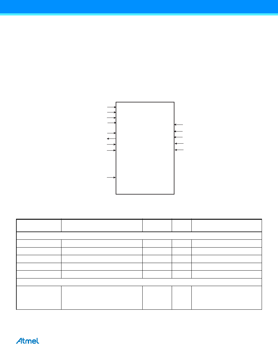
Figure 20-7. Serial Programming
TDI
TDO
TMS
TCK
XIN
TST
VDDIO
PGMEN0
PGMEN1
0-50MHz
VDDIO
VDDCORE
VDDIO
VDDPLL
VDDFLASH
GND
VDDIO
GND
PGMEN2
Table 20-20. Signal Description List
Signal Name
Function
Type
Active
Level
Comments
Power
VDDFLASH
Flash Power Supply
Power
VDDIO
I/O Lines Power Supply
Power
VDDCORE
Core Power Supply
Power
VDDPLL
PLL Power Supply
Power
GND
Ground
Clocks
XIN
Main Clock Input.
This input can be tied to GND. In this
case, the device is clocked by the internal
RC oscillator.
Input
32 kHz to 50 MHz
发布紧急采购,3分钟左右您将得到回复。
相关PDF资料
PIC16C63A-04I/SO
IC MCU OTP 4KX14 PWM 28SOIC
52559-2270
CONN FFC 22POS .5MM VERT ZIF SMD
52559-1870
CONN FFC 18POS .5MM VERT ZIF SMD
DSPIC33EP64MC506-I/PT
IC DSC 16BIT 64KB FLASH 64TQFP
52745-1896
CONN FFC 18POS .5MM R/A ZIF SMD
PIC16LC622-04/P
IC MCU OTP 2KX14 COMP 18DIP
PIC16LF84A-04/P
IC MCU FLASH 1KX14 EE 18DIP
DSPIC30F1010-30I/MM
IC DSPIC MCU/DSP 6K 28QFN
相关代理商/技术参数
PIC16C63A-04I/SS
功能描述:8位微控制器 -MCU 7KB 192 RAM 22 I/O RoHS:否 制造商:Silicon Labs 核心:8051 处理器系列:C8051F39x 数据总线宽度:8 bit 最大时钟频率:50 MHz 程序存储器大小:16 KB 数据 RAM 大小:1 KB 片上 ADC:Yes 工作电源电压:1.8 V to 3.6 V 工作温度范围:- 40 C to + 105 C 封装 / 箱体:QFN-20 安装风格:SMD/SMT
PIC16C63A04SP
制造商:MICROCHIP 功能描述:NEW
PIC16C63A-20/SO
功能描述:8位微控制器 -MCU 7KB 192 RAM 22 I/O RoHS:否 制造商:Silicon Labs 核心:8051 处理器系列:C8051F39x 数据总线宽度:8 bit 最大时钟频率:50 MHz 程序存储器大小:16 KB 数据 RAM 大小:1 KB 片上 ADC:Yes 工作电源电压:1.8 V to 3.6 V 工作温度范围:- 40 C to + 105 C 封装 / 箱体:QFN-20 安装风格:SMD/SMT
PIC16C63A-20/SP
功能描述:8位微控制器 -MCU 7KB 192 RAM 22 I/O RoHS:否 制造商:Silicon Labs 核心:8051 处理器系列:C8051F39x 数据总线宽度:8 bit 最大时钟频率:50 MHz 程序存储器大小:16 KB 数据 RAM 大小:1 KB 片上 ADC:Yes 工作电源电压:1.8 V to 3.6 V 工作温度范围:- 40 C to + 105 C 封装 / 箱体:QFN-20 安装风格:SMD/SMT
PIC16C63A-20/SP
制造商:Microchip Technology Inc 功能描述:8 Bit Microcontroller Clock Speed:20MHz
PIC16C63A-20/SS
功能描述:8位微控制器 -MCU 7KB 192 RAM 22 I/O RoHS:否 制造商:Silicon Labs 核心:8051 处理器系列:C8051F39x 数据总线宽度:8 bit 最大时钟频率:50 MHz 程序存储器大小:16 KB 数据 RAM 大小:1 KB 片上 ADC:Yes 工作电源电压:1.8 V to 3.6 V 工作温度范围:- 40 C to + 105 C 封装 / 箱体:QFN-20 安装风格:SMD/SMT
PIC16C63A-20E/SO
功能描述:8位微控制器 -MCU 7KB 192 RAM 22 I/O RoHS:否 制造商:Silicon Labs 核心:8051 处理器系列:C8051F39x 数据总线宽度:8 bit 最大时钟频率:50 MHz 程序存储器大小:16 KB 数据 RAM 大小:1 KB 片上 ADC:Yes 工作电源电压:1.8 V to 3.6 V 工作温度范围:- 40 C to + 105 C 封装 / 箱体:QFN-20 安装风格:SMD/SMT
PIC16C63A-20E/SP
功能描述:8位微控制器 -MCU 7KB 192 RAM 22 I/O RoHS:否 制造商:Silicon Labs 核心:8051 处理器系列:C8051F39x 数据总线宽度:8 bit 最大时钟频率:50 MHz 程序存储器大小:16 KB 数据 RAM 大小:1 KB 片上 ADC:Yes 工作电源电压:1.8 V to 3.6 V 工作温度范围:- 40 C to + 105 C 封装 / 箱体:QFN-20 安装风格:SMD/SMT